The leading edge of semiconductor manufacturing is a race measured in nanometers and months. TSMC, the world's largest contract chipmaker, has been shipping its N2 2 nanometer node in volume, and attention has already shifted to the next step: the A14 process, which produces 1.4 nanometer class chips. On September 25, 2026, Taiwanese media reported that TSMC has started pilot production of A14 at Fab 20 in Hsinchu Science Park's Baoshan site and at Fab 25 in the Central Taiwan Science Park in Taichung. The reports, which circulated through outlets including UDN, Commercial Times, MoneyDJ, and were later picked up by TechPowerUp, TweakTown, and TrendForce, describe a node that is moving faster than expected.
A14 is not a simple shrink of N2. It is an entirely new process built on second generation gate all around nanosheet transistors and a new standard cell architecture called NanoFlex Pro. That architectural shift separates A14 from A16, which belongs to the 2 nanometer family as a sub node. The distinction matters because TSMC is positioning A14 as its first true angstrom era offering, and the company has publicly said the node should deliver 10 to 15 percent higher performance at the same power, or 25 to 30 percent lower power at the same speed, compared with N2. Logic density is expected to rise by more than 20 percent. Those figures come from TSMC's own disclosures and have been repeated across the Taiwanese technology press.
The geography of the launch is equally important. Pilot production is happening at two sites. Fab 20 in Baoshan, Hsinchu, is TSMC's most advanced development fab, where the company typically proves out new nodes before moving them to larger facilities. Fab 25 in Taichung is the main production hub for A14, and it is still under construction. According to reports, Fab 25 is slated for completion in the second quarter of 2027, with pilot runs potentially starting as early as the third quarter of 2027. Combined A14 capacity at Fab 20 and Fab 25 is expected to reach around 60,000 to 70,000 wafers per month. TSMC has also said it plans to eventually introduce A14 at Fab 22 in Kaohsiung and Fab 21 in the United States.
The competitive context is just as significant. Intel is racing toward its own 14A node on a similar timeline. Intel Foundry chief Naga Chandrasekaran has said the company expects its 14A to be within 5 percent of TSMC's A14. Intel plans to start 14A risk production in the second half of 2027, with high volume production expected in 2028. That puts both foundries on a collision course through 2027 and into 2028, with Samsung also in the mix. The A14 pilot production news is therefore not just a technical milestone. It is a signal about which company may set the pace in the next generation of leading edge chips.
Key Facts
TechPowerUp reported on September 25, 2026 that TSMC's A14 node, which produces 1.4 nanometer chips, has reportedly begun pilot production runs at Hsinchu Science Park's Baoshan Fab 20 and Central Taiwan Science Park's Fab 25. According to UDN, TSMC is conducting pilot production to evaluate the viability of the semiconductor node, allowing customers to see how their potential designs will perform in TSMC's production environment. The reports describe the progress as better than expected, with timelines moving forward because of early success.
TweakTown reported on September 25, 2026 that yields on A14 are apparently running ahead of schedule. Test vehicles are said to be hitting close to 90 percent of target device performance, and 256 megabit SRAM yields are reportedly nearing 90 percent as well. That is a solid position for a node still a couple of years away from mass production, though yield figures this early can still shift. The same reports say A14 is on track to enter trial production in 2027, with pilot production already starting at Fab 20 before shifting to Fab 25 in Taichung. Mass production remains targeted for 2028, in line with what TSMC has said publicly.
TrendForce reported on September 22, 2026 that Commercial Times, citing IC design sources, says pilot production at Baoshan, Hsinchu, could begin as early as the first quarter of 2027, nearly matching Intel's timeline for bringing 14A into production. TrendForce also noted that TSMC launched its A14 CyberShuttle service in the second quarter of 2026 and is expected to begin pilot production at Fab 20. Fab 25 in Taichung, the node's main production hub, is slated for completion in the second quarter of 2027, with pilot runs potentially starting as early as the third quarter of 2027. On process maturity, Intel's 14A defect density had fallen to 0.5 by June 2026, with D0 targeted at 0.1 to 0.2 by the first quarter of 2027.
Intel's Foundry chief, Naga Chandrasekaran, spoke with investment bank KeyBanc Capital Markets about Intel Foundry and the future trajectory of its nodes. TechPowerUp reported on September 25, 2026 that Intel expects its 14A node to be within 5 percent of TSMC's A14. The within 5 percent figure could imply a 5 percent advantage, a 5 percent disadvantage, or a mix of both, so the technical specifics remain uncertain. Intel plans to start 14A node risk production in the second half of 2027, with high volume production expected in 2028. The company has processed tens of thousands of 14A wafers in pilot production runs and is now working on yield improvements and minor node adjustments before beginning risk production next year.
TSMC's A14 process promises up to 15 percent higher speeds at the same power level or up to 30 percent power reduction at the same frequency compared with N2, plus a 20 percent increase in logic density. The node uses second generation gate all around nanosheet transistors and the NanoFlex Pro standard cell architecture. TSMC will continue to use Low NA EUV lithography for A14, as it only plans to transition to High NA around its 1 nanometer node. A follow up node called A13 is also planned, offering a further 6 percent reduction in die area over A14, with volume production expected in 2029.
Analysis
The pilot production milestone is more than a routine update on a roadmap. What this really means is that TSMC is pulling its most advanced node forward at a moment when its main rivals are still trying to prove they can execute. The reported yield figures, with test vehicles near 90 percent of target device performance and 256 megabit SRAM yields approaching 90 percent, suggest that A14 is not just a paper specification. Those numbers are early, and early yield data can change, but they indicate that the process is behaving well enough to move into pilot runs ahead of schedule. For a node that is not expected to reach high volume manufacturing until 2028, that is a meaningful signal of maturity.
The bigger picture here is that the foundry race is no longer only about transistor density. It is about time to market, customer trust, and the ability to absorb enormous capital costs while keeping yields under control. TSMC's decision to run pilot production at Fab 20 in Hsinchu before shifting to Fab 25 in Taichung follows a familiar playbook, but the speed is notable. The company is also extending A14 to Fab 22 in Kaohsiung and Fab 21 in the United States, which shows that this is a global capacity story, not just a Taiwan story. Intel, meanwhile, is trying to close the gap with 14A, and Naga Chandrasekaran's comment that Intel expects to be within 5 percent of TSMC's A14 is a carefully worded claim. It could mean parity, it could mean a slight deficit, and it could mean a slight lead. The ambiguity is deliberate, but it also reveals that Intel sees TSMC as the benchmark.
The yield comparison is worth watching closely. Intel's 14A defect density was reported at 0.5 by June 2026, with a target of 0.1 to 0.2 by the first quarter of 2027. TSMC's reported SRAM yields near 90 percent are not directly comparable to defect density, but they point in the same direction: both companies are making progress. The difference is that TSMC has already started pilot production, while Intel is still working on yield improvements before risk production next year. That gap may be small in calendar terms, but in the foundry business, a few months can determine which company wins the first wave of high volume customers in smartphones, high performance computing, and artificial intelligence.
Another factor is the architecture. A14 is built on second generation gate all around nanosheet transistors and NanoFlex Pro standard cells. That is a departure from A16, which stays within the 2 nanometer family. By making A14 an entirely new process, TSMC is asking customers to adopt a new design ecosystem at the same time that it asks them to trust a new node. The A14 CyberShuttle service, launched in the second quarter of 2026, is part of that effort. It gives customers an early way to test their designs, and the reports say new design tape outs are running ahead of schedule. Strong engagement from smartphone, HPC, and AI customers suggests that demand is not the problem. Execution is.
Why It Matters
For the wider technology industry, A14 matters because it will define the performance and power characteristics of the next generation of chips. Everything from flagship smartphones to data center accelerators depends on the leading edge. The promised gains over N2, including 10 to 15 percent higher speed at the same power or 25 to 30 percent lower power at the same speed, plus more than 20 percent logic density, translate into real product differences. A phone that runs cooler, a server that consumes less electricity, or an AI accelerator that packs more compute into the same area: these are the outcomes that customers care about, and they are the reason TSMC's schedule is watched so closely.
The competitive stakes are equally high. Intel's 14A node is designed to offer a 15 to 20 percent performance improvement at the same power compared with Intel 18A, or a 25 to 35 percent power reduction at the same performance, with up to a 30 percent improvement in chip density. If Intel can hit those numbers and stay within 5 percent of TSMC's A14, it will have a credible answer to TSMC's leading edge. If it cannot, TSMC will extend its dominance. The pilot production news suggests TSMC is not waiting to find out. It is moving first, and it is moving faster than expected.
There is also a geopolitical dimension. TSMC's leading edge production remains concentrated in Taiwan, even as the company expands to the United States with Fab 21. The A14 pilot runs at Fab 20 and Fab 25 are a reminder that Taiwan remains the center of gravity for the most advanced semiconductor manufacturing. Plans to extend A14 to Kaohsiung and Arizona show that TSMC is thinking about geographic diversification, but the first and most important ramp will happen at home. For governments and customers worried about supply chain resilience, that is both reassuring and a source of risk.
Next Up
The immediate next step is risk production, which is scheduled for 2027. If the pilot production proceeds smoothly without major yield or production issues, TSMC may even advance the production schedule by a few months. TrendForce reported that pilot production at Baoshan could begin as early as the first quarter of 2027, and Fab 25 in Taichung is slated for completion in the second quarter of 2027. The company will also continue to develop A13, which is expected to offer a further 6 percent reduction in die area over A14 and reach volume production in 2029.
For Intel, the next year will be about proving that 14A can reach risk production in the second half of 2027 and volume production in 2028. Naga Chandrasekaran's claim that Intel expects to be within 5 percent of TSMC's A14 will be tested in the same window. Both companies are targeting 2028 for high volume manufacturing, and both are pushing their timelines forward. The race is tight, and the pilot production reported on September 25, 2026 is the starting gun for the final sprint.
Related Articles
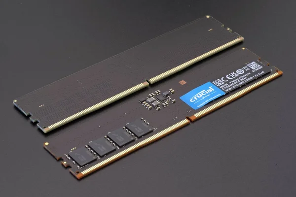
XMG and Schenker Raise Laptop Prices by Up to EUR 300 as DDR5 Memory Costs Surge Sixfold
Schenker and its XMG brand will charge EUR 100 to EUR 300 more for most laptops after DDR5 SO-DIMM modules reached roughly six times their mid 2025 prices, and the firm expects the memory shortage to run into 2027.
Micron Discontinues 2GB GDDR7 Chips, Only 3GB Modules Remain for RTX 50 GPUs
Micron has marked its 2GB GDDR7 memory chips as end of life, leaving only 3GB modules and raising questions about supply for Nvidia's GeForce RTX 50 series GPUs.
Micron Ends 2GB GDDR7 Production Leaving Nvidia RTX 50 Series With Two Memory Suppliers
Micron has designated both of its 2GB GDDR7 parts as End of Life, trimming Nvidia's RTX 50 memory supply base to Samsung and SK hynix while its 3GB modules remain in production.
Comments (0)
Log in or sign up to leave a comment.
No comments yet. Be the first to share your thoughts.