Taiwan broke ground on the Baipu Industrial Park in Kaohsiung on September 21, 2026, a nearly 89 hectare site where Taiwan Semiconductor Manufacturing Company (TSMC) will build two facilities dedicated to technology validation and talent training for advanced integrated circuit packaging. The ceremony marks the start of a project that Kaohsiung officials and the national government describe as a critical piece of the island's semiconductor ecosystem, one that shifts attention from wafer fabrication alone to the packaging steps that turn bare chips into systems capable of powering artificial intelligence.
The park covers 88.73 hectares (219.2 acres), of which about 53.6 hectares are designated for industrial use. Roughly 25 hectares are being positioned for advanced back-end semiconductor equipment and related supply chain companies, according to the Kaohsiung City Government. TSMC, the world's largest contract chipmaker, will occupy a 3 hectare site with two buildings: a technology validation laboratory and a talent training centre. Operations there are expected to begin in the fourth quarter of 2029, while the full park infrastructure is scheduled for completion in 2031.
President Lai Ching-te attended the groundbreaking and framed the project as a response to a global shift. "With the rapid development of AI and high-performance computing, advanced packaging has become a critical part of global semiconductor competition," he said. Lai added that the park would let key equipment and materials suppliers conduct research, testing and validation on site, shortening the time needed to bring new technologies into mass production and helping local companies enter the advanced chipmaking supply chain.
The Baipu park is part of a broader push to build a more complete semiconductor ecosystem in southern Taiwan, complementing TSMC's advanced chipmaking operations at the nearby Nanzih Technology Industrial Park. Taiwan is home to the world's largest semiconductor manufacturing industry and a broad network of chip equipment, materials, testing and packaging suppliers. Government and city officials have been seeking to expand that network in the south, where TSMC, ASE Technology Holding and Foxconn are increasing investment.
Key Facts
Reuters reported on September 21, 2026, that TSMC will build two buildings at Baipu Industrial Park, including a technology validation laboratory and a talent training centre. Kaohsiung Deputy Mayor Lo Ta-sheng described those plans at the groundbreaking ceremony. The facilities are expected to begin operations in the fourth quarter of 2029.
Focus Taiwan, the English language news service of the Central News Agency, reported on September 21, 2026, that the park is projected to create more than 4,000 jobs and generate about NT$300 billion (US$9.35 billion) in annual production value. President Lai called the project a new milestone for Taiwan's semiconductor industry and said it would strengthen the island's ecosystem, balance north south development and boost global competitiveness.
TechNode Global reported on September 21, 2026, that the park covers 88.73 hectares, including about 53 hectares of industrial land, with around 25 hectares positioned for advanced back-end semiconductor equipment and supply chain firms. The report noted that more than 20 semiconductor related supply chain companies were expected to take part in the groundbreaking.
BigGo Finance reported on September 21, 2026, that the Kaohsiung City Economic Development Bureau received official designation approval for the park from Taiwan's Ministry of Economic Affairs on March 17, 2026. The park will adopt what the city calls a demand side, research and development side and park side collaboration model, connecting existing clusters in Nanzih for advanced manufacturing, Renwu for advanced packaging and testing, and Qiaotou for materials and key components.
According to TSMC, its 3 hectare site will include small cleanrooms and laboratories for testing and joint development of advanced assembly technologies, equipment and materials, as well as a training centre for highly skilled specialists in semiconductor processes and equipment. The buildings will house modular facilities that can be reconfigured as technology evolves. Kaohsiung's Economic Development Bureau said construction of two campuses at the park, including the two TSMC facilities, is scheduled for completion in the fourth quarter of 2029.
Analysis
What this really means is that the global chip industry's centre of gravity is shifting from the wafer to the package. For decades, Moore's Law rewarded companies that could shrink transistors. As those gains slow and costs rise, the industry is instead stacking multiple dies, memory and other components inside tightly integrated packages. That approach, known broadly as advanced packaging, is how designers such as Nvidia, Advanced Micro Devices and Broadcom build the accelerators that train and run AI models. TSMC's advanced packaging technology is used to produce those chips.
The bottleneck has become capacity for packaging, not just for making the leading edge transistors. TSMC's CoWoS advanced packaging capacity is seen doubling from 130,000 wafers per month at the end of 2026 to 260,000 by the end of 2028, a trajectory that explains why Taiwan is willing to devote public land and infrastructure to a park focused on equipment, materials, validation and training rather than on another wafer fab. Baipu is designed to speed up the qualification of the tools and chemicals that packaging lines need, a step that can otherwise take years.
The bigger picture here is that Taiwan is trying to defend a strategic advantage by deepening its ecosystem rather than simply adding more manufacturing lines. The park aims to become Taiwan's first semiconductor base focused on developing, testing and certifying critical semiconductor equipment and raw materials, according to President Lai. If suppliers can validate their products at Baipu, they can move more quickly into mass production for TSMC and its peers. That helps local metal processing and precision machinery companies integrate into a high value added supply chain, as the city's Economic Development Bureau has argued.
Liao Tai-hsiang, Director General of Kaohsiung's Economic Development Bureau, said that with advanced packaging demand growing rapidly in the post Moore's Law era, Baipu will become a critical node in the next phase of the Southern Taiwan Semiconductor S Corridor. The corridor links Chiayi, Tainan, Kaohsiung and Pingtung, and Baipu is meant to complement the packaging and testing cluster at Renwu Industrial Park and the materials cluster at Ciaotou Science Park. Market sources indicate that Deputy Mayor Lo Ta-sheng and TSMC Vice President of Advanced Packaging Technology and Service He Jun recently exchanged views on industry needs and the park's future development.
Why It Matters
Advanced packaging has become the stage on which AI compute is won or lost. AI accelerators and high performance computing systems increasingly combine multiple dies, memory and other components within tightly integrated packages, raising the importance of packaging equipment, materials, validation and manufacturing capacity alongside leading edge wafer fabrication. A shortage of packaging capacity can idle the most advanced chips, which is why TSMC has been expanding CoWoS output so aggressively.
For Taiwan, the project is also about geography and resilience. The government has been seeking to spread semiconductor investment beyond the northern Hsinchu region, and Kaohsiung has become a second pole. TSMC is already building advanced chipmaking operations at Nanzih, while ASE Technology Holding and Foxconn are increasing investment in the south. Baipu adds a layer that is explicitly about the supply chain that feeds those factories, from precision machinery to cleaning chemicals and testing services.
Infrastructure questions remain part of the story. President Lai said the government had assessed Taiwan's electricity needs through 2035 and that there would be no problem maintaining a stable supply. On water, he cited a pearl string project that connects reservoirs through interregional pipelines. State owned Taiwan Power Co. has agreed to build a distribution network in the park, according to Focus Taiwan. Those commitments matter because semiconductor packaging and testing facilities are power and water intensive.
Next Up
With the groundbreaking complete, attention turns to construction and tenant recruitment. The Kaohsiung City Government will build factory facilities, while TSMC develops its own 3 hectare site. The two TSMC buildings and two campuses are due for completion in the fourth quarter of 2029, and the park's entire infrastructure is expected to be finished in 2031. More than 20 supply chain companies attended the ceremony, and the city is now seeking to convert that interest into signed investment.
The broader test is whether Baipu can shorten the path from laboratory validation to mass production for advanced packaging tools and materials. If it does, Taiwan will have added a new kind of semiconductor asset to its portfolio, not another fab but a proving ground for the equipment and chemicals that keep the fabs and packaging lines running.
Related Articles
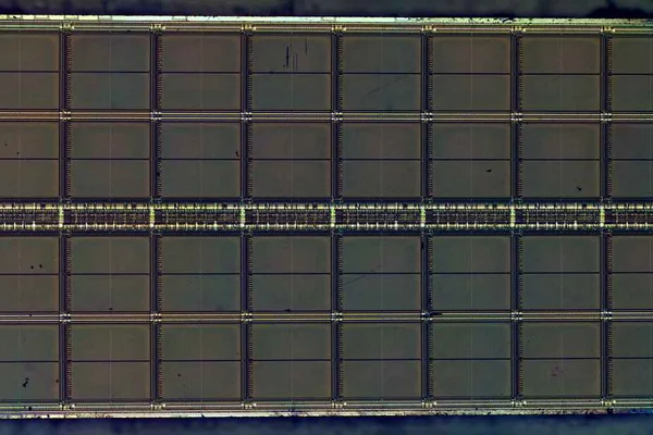
CXMT puts fifth-generation DRAM platform into mass production without EUV tools
ChangXin Memory Technologies says its G5 DRAM platform reaches an 11.95 nanometre active-area half-pitch using quadruple patterning, claiming a process leap achieved without EUV lithography.
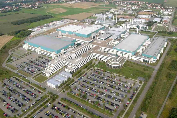
Japan and US discuss ¥3 trillion GlobalFoundries logic chip fab under $550 billion pledge
Japan and the United States are negotiating a ¥2 trillion to ¥3 trillion logic chip factory on American soil that GlobalFoundries would operate under a $550 billion investment pledge, Nikkei reported.
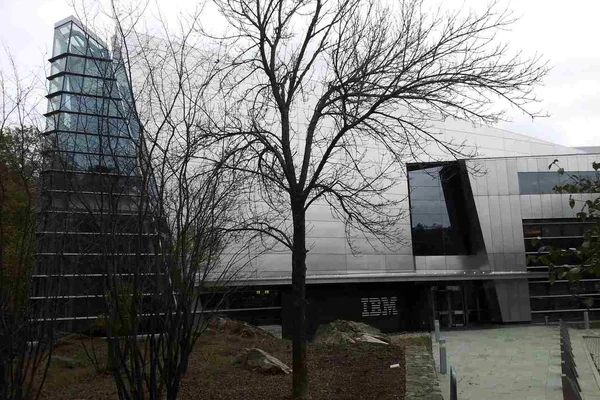
IBM's Anderon finalizes $1 billion CHIPS Act award for Albany quantum chip foundry
Anderon LLC, an IBM subsidiary, has locked in a $1 billion federal award for a 300 millimeter quantum wafer foundry in Albany, New York, with first wafers already in production.
Comments (0)
Log in or sign up to leave a comment.
No comments yet. Be the first to share your thoughts.