For three decades the Onyang campus in South Chungcheong Province has been the quiet back end of Samsung Electronics' memory business, a site where conventional semiconductors were assembled, tested and shipped rather than designed or patterned. Onyang began as a semiconductor assembly and testing line in 1991, and for most of its history it sat at the lower-margin end of a business whose prestige and profit were concentrated in front-end wafer fabrication at Pyeongtaek and elsewhere in South Korea.
That division of labor is now being rewritten. On November 12, 2026, Samsung Electronics broke ground on Onyang Line 5, the first of five high-bandwidth memory packaging lines planned for its Asan campus, under a total investment of 46 trillion won, or about US$34.5 billion. The company is targeting operations at the new plant in June 2028, roughly a year ahead of the original schedule.
The ceremony, attended by Chairman Lee Jae-yong, was part of a government initiative to develop the central Chungcheong region into a global hub for AI-driven innovation. It also marked the first construction start among the large Samsung projects announced for the region, which together cover advanced memory packaging, OLED display panels and semiconductor package substrates.
Advanced packaging has moved from a footnote to a bottleneck in the AI supply chain. Seoul Economic Daily reported on November 12, 2026 that Samsung shortened construction of Line 5 by one year to meet what it called explosive growth in demand for server memory. The plant is designed to take DRAM dies that have completed front-end processing in Pyeongtaek and put them through back-end steps such as stacking, bonding and inspection at Onyang, which is why a site once associated with mature products is now being recast as the heart of AI semiconductors.
Key Facts
Yonhap reported on November 12, 2026 that Chairman Lee Jae-yong pledged to turn the site into a major hub for advanced chip packaging, including high-bandwidth memory. Once focused primarily on the basic assembly and testing of conventional semiconductors, Lee said, the site will transform into a key hub for cutting-edge HBM, the heart of AI semiconductors. The remarks were made at the groundbreaking ceremony in Onyang, South Chungcheong Province.
The 46 trillion won figure divides into 6 trillion won of construction spending and 40 trillion won of advanced equipment, deployed in phases across the campus. Line 5 itself accounts for an initial 6 trillion won, according to Seoul Economic Daily, and consists of a three-story building with a cleanroom of 31,000 square meters, or about 9,400 pyeong, dedicated to advanced HBM production.
Once the buildout is complete, the campus total floor space is expected to expand to 420,000 square meters from 270,000 square meters, an increase of roughly 1.6 times, and the facility is expected to create about 700 direct jobs. Seoul Economic Daily put the wider economic impact of Samsung's Chungcheong spending at 17.3 trillion won, with 11,000 new hires including partner companies, a figure that matters because most of the employment sits with suppliers rather than on the fab floor.
TrendForce reported on November 12, 2026, citing Chosun Biz, Asia Business Daily, Yonhap and Seoul Economic Daily, that Line 5 will produce next-generation HBM including seventh-generation HBM4E, with operations moved up by about one year to June 2028. Asia Business Daily reported that HBM mass production at the site is expected to begin in May 2029, a reminder that starting a fab and filling it are different milestones.
The project sits inside a much larger regional commitment. Seoul Economic Daily reported on November 12, 2026 that four Samsung affiliates will invest a combined 144 trillion won, or about US$98 billion, in Chungcheong, up 4 trillion won from the 140 trillion won announced in July 2026. Samsung Electronics accounts for 60 trillion won of that total, up from 56 trillion, while Samsung Display contributes 67 trillion won, Samsung Electro-Mechanics 8 trillion won and Samsung SDI 9 trillion won. TrendForce reported on November 12, 2026 that, according to Reuters, President Lee said the chip packaging expansion would spur about US$30 billion.
Analysis
The headline number is the 46 trillion won, but the more revealing figure is the 40 trillion won earmarked for equipment. What this really means is that Samsung is not buying real estate or cleanroom shell space so much as it is pre-purchasing a position in the back end of AI memory, where stacking, bonding and inspection determine how many usable HBM stacks leave the building. Construction is the cheaper and more predictable part. Tools are the expensive and contested part, and phasing them lets Samsung slow or accelerate without abandoning the site.
The one-year pull-forward also tells a story about competitive pressure. Samsung raised its Chungcheong plan from 140 trillion won to 144 trillion won only months after announcing it in July 2026, and lifted the electronics piece from 56 trillion won to 60 trillion won. Maeil Business Newspaper reported on November 12, 2026 that Line 5 is scheduled to begin operations in June 2028, at least a year ahead of the original plan, and that HBM4E is expected to become a mainstay for Samsung Electronics and SK hynix starting next year. A schedule change of that size, disclosed months after the original plan, reads as a signal about customers as much as about construction crews.
The demand backdrop is the justification Samsung will point to. Maeil Business Newspaper cited market research firm Yole Group forecasting that the global market for high-performance semiconductor packaging will grow at least fourfold, from US$12.1 billion last year to US$51 billion in 2031. The bigger picture here is that packaging, long treated as the low-value tail of the semiconductor chain, is being repriced as the step that decides who can ship AI memory at volume.
There is a credible counterargument. June 2028 is an operations target, while mass production is reported for May 2029, and a cleanroom of 31,000 square meters does not by itself guarantee yields on a seventh-generation product. Samsung's own language, with Vice Chairman Jun Young-hyun crediting administrative support from central and local governments for the speed of construction, suggests that permitting and site work were the binding constraint rather than process maturity. The schedule is impressive, but it is a construction schedule first, and the market will only learn the difference when tools are qualified.
Why It Matters
Onyang is a test of whether Samsung can convert a legacy assembly site into a strategic asset at the exact moment AI servers are straining memory supply. If Line 5 runs as planned and the remaining four lines follow, the campus becomes a single location where all five lines handle HBM packaging, giving Samsung something competitors cannot replicate quickly: co-located capacity that can be reallocated between generations without rebuilding a supply chain. Chairman Lee has visited the Cheonan plant in June and Samsung's Advanced Package Lab in Yokohama, Japan, in November, which is consistent with a leadership that is treating packaging as a product line rather than a service.
The regional dimension matters too. The ceremony was framed as part of a government initiative to turn the central Chungcheong region into a global hub for AI-driven innovation, and the affiliate breakdown shows how that is meant to work in practice. Samsung Display's A7 OLED line in Asan, funded at 5.9 trillion won with 562,000 square meters of floor area, began construction in October and targets mass production in the second half of 2029. Samsung Electro-Mechanics' new Sejong substrate plant, 4.3 trillion won of its 8 trillion won total, targets mass production in September 2028. The three projects are staggered across 2028 and 2029.
For the wider supply chain, the numbers that matter are 420,000 square meters, 700 direct jobs and 11,000 hires including partner companies. Those are modest against the capital totals, which is precisely the point. Advanced packaging is a capital-intensive, relatively labor-light business, and the economic return depends on tool utilization rather than headcount, so the regional payoff will show up in supplier clusters and in the substrate and materials ecosystem around Asan and Cheonan rather than in a single employment figure.
Next Up
Attention now shifts to execution milestones. Groundwork is already under way at Onyang, and the first real test will be equipment move-in and qualification ahead of the June 2028 operations target, followed by the reported May 2029 start of HBM mass production. Samsung has said it will link Onyang and Cheonan and develop Chungcheong into a global hub for advanced packaging, a plan Vice Chairman Jun Young-hyun has repeated publicly.
The four remaining Onyang lines, the Asan A7 OLED build and the Sejong substrate plant give the region a staggered pipeline running through 2029. If those dates hold, Samsung will have converted a site that has assembled conventional chips since 1991 into the physical center of its AI memory ambitions, and it will have done so a year earlier than it originally told the market.
Related Articles
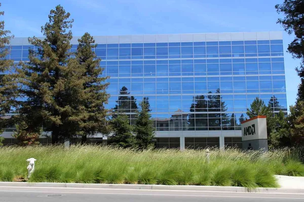
AMD ships 6th Gen EPYC 9006 Venice server chips with 256 cores on TSMC 2nm
The 256 core flagship EPYC 9996 leads a lineup that stretches from $14,904 down to $700, with AMD claiming up to 3.7x the performance of Nvidia's Vera CPU.
TSMC Posts Record NT$586.89 Billion October as AI Demand Keeps Advanced Nodes Full
The Taiwanese foundry's October revenue rose 59.7 percent year on year to a company record, with demand for leading-edge chips accelerating as AI infrastructure spending climbs.
ASML Supply Shortfall Pushes Samsung and SK hynix Into an EUV Delivery Slot Race
Memory makers are racing to lock in lithography capacity years ahead of need, and the scramble is already reshaping capital spending plans across South Korea.
Comments (0)
Log in or sign up to leave a comment.
No comments yet. Be the first to share your thoughts.